


Introduction to SMT Assembly
Surface Mount Technology (SMT) has revolutionized electronics manufacturing since its widespread adoption in the 1980s. Unlike through-hole technology, SMT components are mounted directly onto the surface of printed circuit boards (PCBs), allowing for higher component density, improved performance, and automated production.
This comprehensive guide will walk you through each step of the SMT assembly process, highlighting key considerations, equipment used, and quality control measures at each stage. Whether you’re new to electronics manufacturing or looking to deepen your understanding of modern PCB assembly, this article provides valuable insights into one of the most critical processes in electronics production. Quick Facts About SMT
- SMT allows for components to be placed on both sides of a PCB
- Components can be up to 10 times smaller than through-hole equivalents
- Modern SMT lines can place over 100,000 components per hour
- SMT was first developed in the 1960s but didn’t see widespread use until the 1980s
- Over 90% of electronic devices today use SMT assembly
Step 1: Solder Paste Printing
The first step in the SMT assembly process is applying solder paste to the PCB. Solder paste is a mixture of tiny solder particles suspended in flux medium. It’s applied only to the areas where components will be placed – specifically, the component pads.
This process uses a stencil (or solder mask) – a thin metal sheet with precisely cut openings that correspond to the PCB pads. The stencil is aligned with the PCB, and a squeegee blade spreads solder paste across the stencil, forcing it through the openings onto the PCB pads.
Key Considerations:
- Stencil Design: Thickness and aperture size affect paste volume
- Paste Viscosity: Affects printing quality and consistency
- Squeegee Parameters: Pressure, speed, and angle impact print quality
- Environmental Control: Temperature and humidity affect paste behavior
After printing, the PCB moves to an automated optical inspection (AOI) system to verify the quality and accuracy of the solder paste application. Any defects at this stage can lead to serious issues later in the process, making this a critical quality control point.
For more information on this stage, see our article on Solder Paste Printing Best Practices.
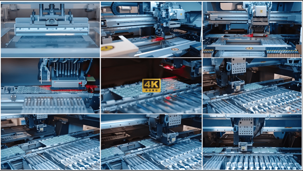
Step 2: Component Placement
Once solder paste is applied, components are precisely placed onto the PCB. This is typically done using high-speed automated placement machines (pick-and-place machines) that can place tens of thousands of components per hour with remarkable accuracy.
Components are supplied on reels, trays, or tubes and are fed into the placement machine. A robotic head picks components using vacuum nozzles, orients them correctly, and places them onto the solder paste on their designated pads. Types of Placement Machines
| Machine Type | Speed | Accuracy | Best For |
|---|---|---|---|
| High-Speed Chip Shooters | Up to 200,000 cph | ±50μm | Small passive components |
| Flexible Placers | Up to 30,000 cph | ±25μm | Mixed component sizes |
| Ultra-High Accuracy | Up to 15,000 cph | ±10μm | Fine-pitch and BGA components |
Placement Challenges:
- Component Miniaturization: 0201 and 01005 components require extreme precision
- Mixed Technology: Placing both SMT and through-hole components
- Thermal Management: Components with different thermal requirements
- Orientation: Polarized components must be placed with correct orientation
After component placement, some manufacturers use a pre-reflow inspection to verify correct component placement before proceeding to soldering.
Step 3: Reflow Soldering
Reflow soldering is the process of melting the solder paste to create permanent electrical and mechanical connections between components and the PCB. The assembled PCB passes through a reflow oven with carefully controlled temperature zones.
The reflow process consists of four main stages:
- Preheat: Gradually raises the temperature to activate the flux
- Soak: Allows the entire assembly to reach a uniform temperature
- Reflow: Temperature exceeds the solder melting point, creating joints
- Cooling: Controlled cooling to form reliable solder joints
Temperature Profile Considerations:
- Peak temperature must exceed solder melting point but remain below component damage thresholds
- Different solder alloys (SnPb, SAC305) require different profiles
- Board thickness and component density affect heat distribution
- Thermally massive components may require special considerations
Modern reflow ovens use multiple heating zones (typically 6-12) with precise temperature control and convection heating for even heat distribution. Nitrogen atmosphere may be used to reduce oxidation and improve joint quality.
Learn more about temperature profiling in our Reflow Soldering Optimization Guide.
Step 4: Inspection & Testing
After soldering, the assembled PCBs undergo rigorous inspection and testing to ensure quality and functionality. Several inspection methods are commonly used:
Automated Optical Inspection (AOI)
AOI systems use cameras to automatically inspect PCBs for defects such as missing components, misalignment, solder bridges, and insufficient solder. Advanced systems use 3D imaging to measure solder paste volume and joint quality.
X-Ray Inspection
For components with hidden solder joints (like BGAs and QFNs), X-ray inspection is essential. It can reveal voids, insufficient solder, and alignment issues that aren’t visible to optical systems.
In-Circuit Testing (ICT)
ICT uses a bed-of-nails fixture to make contact with test points on the PCB, verifying component values, presence, orientation, and basic functionality of the circuit.
Functional Testing
This final test verifies that the assembled PCB performs its intended function under real or simulated operating conditions. Common SMT Defects
| Defect Type | Causes | Detection Method |
|---|---|---|
| Tombstoning | Uneven heating, pad size mismatch | AOI, Visual Inspection |
| Solder Bridges | Excessive paste, misalignment | AOI, X-Ray |
| Insufficient Solder | Stencil issues, poor paste transfer | AOI, X-Ray |
| Component Shift | Placement accuracy, reflow turbulence | AOI, X-Ray |
| Voids in Solder Joints | Contamination, outgassing | X-Ray |
Step 5: Cleaning & Finishing
The final step in the SMT assembly process involves cleaning and applying protective coatings if required:
PCB Cleaning
Flux residues left after soldering can be corrosive and affect long-term reliability. Cleaning removes these residues using aqueous or solvent-based cleaning systems. The need for cleaning depends on the flux type used (rosin, no-clean, or water-soluble).
Conformal Coating
For electronics that will operate in harsh environments (high humidity, temperature extremes, contaminants), a protective conformal coating may be applied. This thin polymeric film protects against moisture, dust, chemicals, and temperature extremes.
Final Inspection and Packaging
Before shipment, boards undergo a final visual inspection and are packaged according to customer requirements, which may include anti-static packaging, vacuum sealing, or specialized containers for sensitive components.
Advantages of SMT Over Through-Hole Technology
SMT offers numerous advantages that have made it the dominant PCB assembly method:
- Higher Component Density: SMT components are smaller and can be placed on both sides of the board
- Better Performance: Shorter leads reduce parasitic inductance and capacitance
- Cost Efficiency: Lower material costs and highly automated process
- Faster Production: Simultaneous placement of multiple components
- Improved Reliability: Better mechanical performance under vibration
- Design Flexibility: Enables smaller and more complex electronic devices
These advantages explain why SMT has largely replaced through-hole technology in modern electronics manufacturing, particularly for consumer electronics, telecommunications equipment, and computing devices.
Conclusion
The SMT assembly process represents a sophisticated, highly automated manufacturing system that has enabled the electronics revolution of the past few decades. From solder paste printing to final inspection, each step requires precise control and monitoring to ensure high yield and reliability.
As electronic components continue to shrink and performance demands increase, SMT technology continues to evolve with finer pitch capabilities, advanced materials, and increasingly sophisticated inspection systems. Understanding this process is essential for anyone involved in electronics design, manufacturing, or quality assurance.
For more technical information or specific applications, explore our Technical Articles or contact our engineering team through our Support Center.


留下评论